If you want a sine wave oscillator. We have many circuit for you. Now I am going to show you the Wien Bridge Oscillator circuit.
In normal It has low distortion. And can easily adjust the resonance frequency. That depends on the pair of resistors (R) and capacitors (C).
We can calculate the formula.
F = 1/2 p RC
How Wien bridge oscillator works
The first circuit is a simple Wien Bridge Oscillator.
Wien bridge oscillator is a sine wave oscillator. It can generate a big of frequencies.
The oscillator was based on a bridge circuit. Which includes four resistors and two capacitors.
The oscillator can also be viewed as a positive gain amplifier combined with a bandpass filter that provides positive feedback.
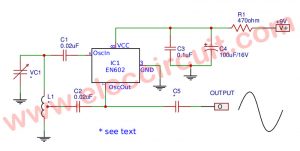
The field-effect transistor (FET) Q1 works in the linear resistive region to give automatic gain control.
For the reduction of the R-C network is one-third at the zero phase-shift tremble frequency.
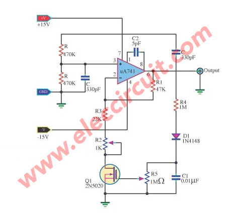
The OP-AMP gain determined by resistor R1 and equivalent resistor RT must be just equal to three to make up the unity gain positive feedback requirement needed for stable oscillation.
Resistors R2 and R3 are set to approximately 1000 ohm less than the required R1 resistance.
The FET – 2N5020 dynamically provides the trimming resistance needed to make RT one-half of the resistance of R1.
The circuit composed of R4, D1, and C1 isolates, rectifies, and filters the output sine wave, converting it into a dc potential to control the gate of the FET.
For the low drain-to-source voltage used, the FET provides a symmetrical linear resistance for a given gate to source voltage.
Assembling
This circuit is not designed for PCB. If you do not want to design own PCB. Or use universal PCB Board that difficult.
Although the circuits are is not the same. It can produce a sine wave signal as well.
#The Second: Wien bridge oscillator Circuit
In this circuit, as Figure 1 the oscillator is based on the R that includes with R1 + P1a (or R2 + P1b), and C is C1, C2 or either C3 (or C4, C5 or C6). And more parts are connected with IC1, IC2 op-amp ICs.
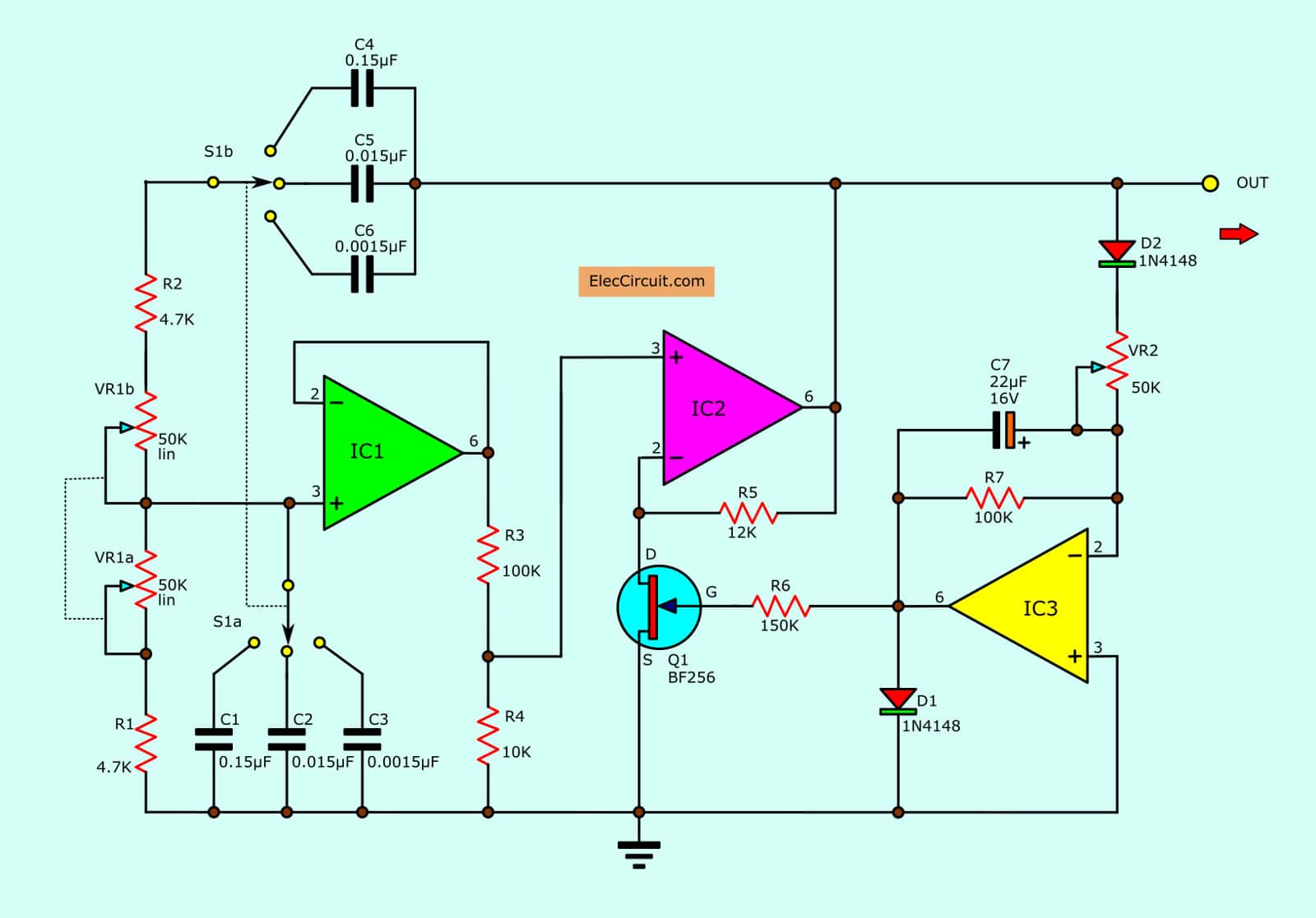
Some output signal from IC2 is sent to the voltage attenuator circuit, that includes of IC3 and T1. The T1 is FET that is used as the variable resistors as the feedback of IC2
The gain of OP-Amp is controlled by the voltage and changing the control voltage of T1 by P2. It needs to tuning to the oscillation to have high efficiency, on the frequency range is selected.
When we use the value of parts as a schematic diagram of the Wien bridge oscillator circuit will have frequencies of about 20 Hz – 22.5 Khz by adjusting P1 and maximum harmonic distortion approximately 2 %.
This circuit requires a Dual voltage (positive-negative) power supply. so we use the voltage converter circuit as Figure 2 input is 9V to +4.5V, Ground, -4.5V.
We use principles like the voltage divider using OP-AMP IC-741 and few parts.
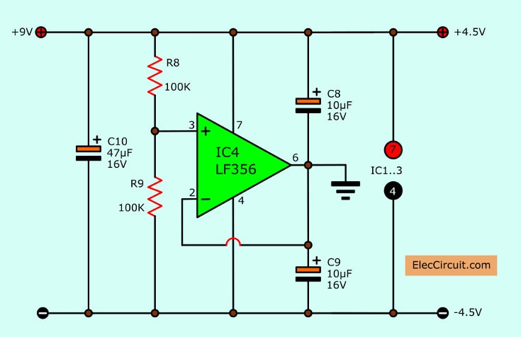
Read more: Power Supply Splitter Circuit using Op-amp
The parts list
IC1-IC3: CA3140, 4.5MHz, Bimos Operational Amplifier With MOSFET Input/bipolar Output.
IC4: LM741, Operational Amplifier
D1,D2: 1N4148, 75V 150mA Diodes
T1: BF256,BF244, FET
P1: 47K, potentiometer
P2: 47K, Pot
Polyester Capacitor
C1,C4: 150nF or 0.15uF 63V
C2,C5: 15nF or 0.015uF 63V
C3,C8: 1.5nF or 0.0015uF 63V
C7: 22uF 16V tantalum capacitors
C10: 47uF 16V, electrolytic
C11,C12: 10uF 16V, electrolytic
1/4W Resistors tolerance: 5%
R1,R2: 4.7K
R3,R7,R8,R9: 100K
R4: 10K
R5: 12K
R6: 150K
SW1: 3 step selector switch
GET UPDATE VIA EMAIL
I always try to make Electronics Learning Easy.
Related Posts

I love electronics. I have been learning about them through creating simple electronic circuits or small projects. And now I am also having my children do the same. Nevertheless, I hope you found the experiences we shared on this site useful and fulfilling.
The first circuit shows a depletion mode n-channel MOSFET. The 2N5020 is in fact a p-channel JFET.
Yes, and the 2N5020 is currently quite expensive. I think any general purpose P-channel depletion mode jfet would work.