The CD4046 is a phase-locked loop (PLL) CMOS IC. Integrated within the CD4046 are two phase comparators and a voltage-controlled oscillator (VCO), both of which have a separate common input.
The CD4046 is commonly used in a variety of applications, including voltage-to-frequency conversion, frequency synthesis and multiplication, signal conditioning, and others. Most people use it for its phase-locked loop (PLL) system.

Basics of Phase-Locked Loop (PLL)
The PLL system functions by a phase comparator comparing an input signal and the center frequency of the VCO, then generating an error voltage proportionate to the difference between an input signal and the VCO frequency. This error voltage passes through an external low-pass filter (LPF) and will then adjust the VCO’s center frequency to match that of the input signal, creating a frequency-feedback system.
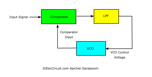
However, the VCO could also be used by itself without being fed through to the phase comparator. Moreover, an LPF part of the PLL consists of an external capacitor and a couple of resistors; often one of the resistors is a potentiometer, meaning that we could variably change the frequency of the VCO on the fly.
Characteristics of CD4046
The CD4046 usually comes in a dual-in-line 16-pin (DIP-16) package. It requires a supply voltage range of 3V to 18V and low power consumption of 70μW (@5V), with low frequency drift of about 0.04% (@10V) and an operating frequency range of up to 1.4MHz (@10V). Meanwhile, the VCO has a high linearity of 1% or less (@10V) and very low standby power consumption.
For more in-depth specifications, see the datasheet.
CD4046 Pinout
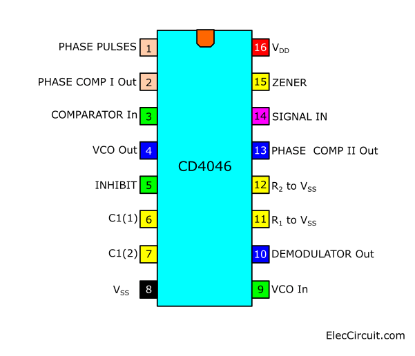
The CD4046 also has two choices of phase comparator available, both of which are driven by the common input. The phase comparator 1 is an exclusive-OR (XOR) network, which works as an overdriven balanced mixer, whereas the phase comparator 2 is an edge-controlled digital memory network that consists of four flip-flops, control gating, and p- and n-drivers with shared output. To oversimplify, in a PLL system, the p- and n-drivers adjust the LPF’s capacitor voltage until the comparator inputs are equal to the signal input.
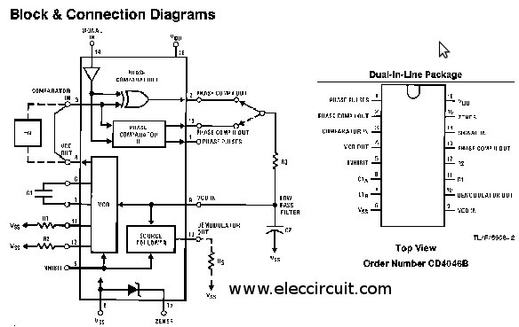
Precaution When Using The CD4046
However, the internal workings of the CMOS IC are complex and frequently offer no practical use. Instead, here are a few points to consider when working on this CD4046 CMOS integrated circuit in particular:
- The voltage at the signal input (pin 14) must not exceed the supply voltage.
- Connect the unused input pins (3, 5, 9, and 14) to the ground or positive voltage supply.
- Disconnect the pins 6, 7, 10, 11, 12, and 15 if the circuit does not call for its use.
- Never connect or disconnect the CMOS chip from or to the circuit while it is running; turn the circuit off completely before doing so.
CD4046 Example Circuits
Now let’s look into some of the example circuits that used the CD4046 as their main component.
100Hz-10KHz Square Wave Signal Generator Circuit Using CD4046
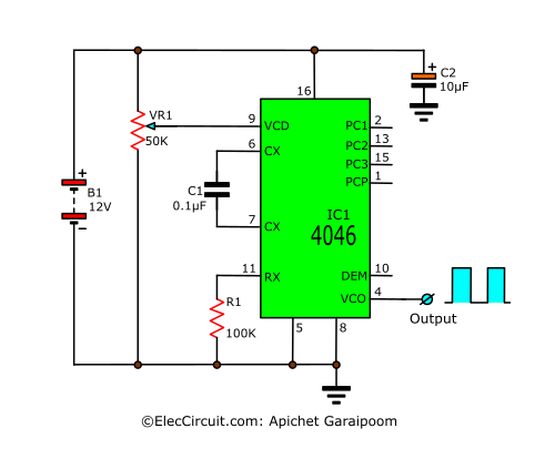
This square wave generator circuit uses the CD4046 as its main component, which is a phase-locked loop (PLL) IC. By only utilizing the voltage-controlled oscillator (VCO), we can effectively use this PLL integrated circuit as a square wave signal generator of any frequency within the range of 1Hz to 1MHz, depending on the external components.
The said external components are VR1 and C1, which together allow us to adjust the voltage going into the oscillator; R1 and R2 determine the highest and lowest frequency of the circuit, respectively, while C2 functions as a filter for the IC1.
How It Works
If the voltage at pin 9 of the IC1 is low, the frequency of the output at pin 4 is also low. In contrast, if the voltage at pin 9 is high, the output frequency at pin 4 will also be high. To put it in a nutshell, the output frequency changes directly correlate with the voltage.
Changing the capacitance of C1 changes the entire output frequency range, so you can choose a value of C1 based on the frequency range listed in the table below.
| C1 (25V) | Frequency Range |
| 1μF | 0 – 100Hz |
| 0.1μF | 10Hz – 1kHz |
| 0.01μF | 100Hz – 10kHz |
Universal tester circuit with VCO(voltage controlled oscillator)
This universal tester circuit can test a variety of electronic components and circuits using the core principle of a VCO. It is capable of testing circuits with high impedance and only consumes a small amount of current of 3mA.
The VCO, or voltage-controlled oscillator, is a circuit that uses the input voltage to control the output frequency. Or in other words, the voltage determines the frequency. It is considered a fundamental of signal wave generators, capable of generating a square, triangular, and sine wave signal.
How It Works
This VCO circuit we are using to test the working of a circuit generates up to around 1.2kHz and uses a testing voltage of 9V.
The testing voltage is coming from a 9V battery that connects directly to one of the probes, which will supply the circuit being tested with input voltage. Meanwhile, the other probe acts as a voltage measurer, measuring the output voltage from the circuit being tested.
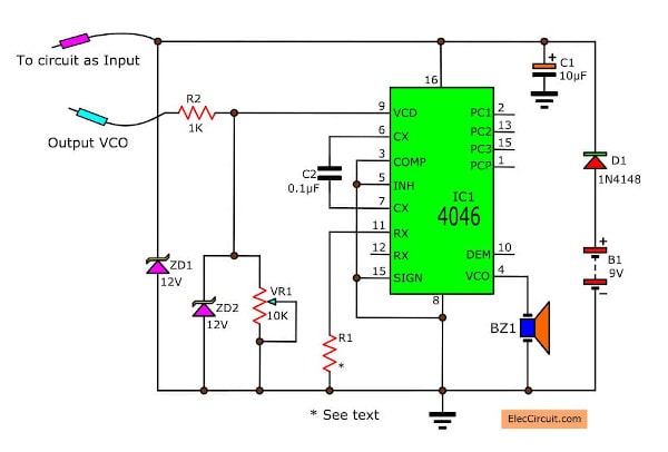
The output probe is connected to pin 9 of IC1, which is the control pin for the VCO circuit. Therefore, if the output probe does not detect any voltage, the VCO will not generate any signal. But if the output probe detects voltage, pin 9 receives voltage, causing the VCO to generate a signal with a maximum of 1.2kHz.
The exact frequency is determined by C1 and R1 and then plays through a BZ1 as an audible noise. When the R1 connects to pin 11, it will control the maximum frequency, whereas when it connects to pin 12, it will control the minimum frequency.
The Zener diodes ZD1 and ZD2 prevent the voltage from entering the input of the VCO. Furthermore, potentiometer VR1 allows us to adjust the testing current, which is useful when testing a circuit with high impedance. In addition, C1 filters the current for the IC1 and prevents reverse polarity power supply.
Building This Circuit
We assemble this circuit on a universal PCB using the layout shown in the illustration below.

Components List
Resistors 0.25W +5%
R1: 5K
R2: 1K
VR1: 10K Potentiometer.
Capacitors
C1: 10uF 16V, Electrolytic
C2: 0.1uF 50V, Polyester
Semiconductor
D1: 1N4148
ZD1, ZD2: 12V 1W
IC1: CD4046
Others
BZ1: Piezo speaker
Two small probes.
PCB universal.
Conclusion
The CD4046 has numerous use cases and applications, and I have yet to try the majority of them; thus, I can only discuss circuits that only use the VCO part of the IC. However, if you have an idea for a circuit that utilizes other aspects of the CD4046 and would like us to cover it, please let us know. Anyway, I hope you find this article useful in some way. Thank you for reading.
GET UPDATE VIA EMAIL
I always try to make Electronics Learning Easy.
I am using the 4046 to run the 4017 I want it to count 1-2-3 and repeat 1-2-3 but I get a clock pules between the repeats, this I don’t want. I can’t find the problem. The 4046 works very good. Can you sow or send? a lay out of the 4017 to do this. Thank You.
Jerry
PS.
The pin # and the output # are confusing, maybe that’s my problem.
I’m glad you can use the CD4046 well. Because my English is pretty bad, I don’t understand the meaning clearly. Do you want to use CD4017? Let’s try this: https://www.eleccircuit.com/led-chaser-circuit/
When you get the result. Please let me know. Thanks.
Overall, as a DJ, a SoundCloud downloader is an invaluable tool that helps me deliver a unique and exciting musical experience to my audience.
I guess the pins #4 and #11 are swapped inadvertently on Fig. 1.
Thank you for your feedback.
And what about pin 10 (Demodulator output) for use in a circuit?
I am using CD4046 along with CD4029 to build a frequency multiplier by 4.
Input is PWM signal with duty cycle 80% and frequency range is 130 Hz to 380 Hz.
Kindly advise.
It’s great! The author spent a lot of time and thought, and the content is completely dry goods. I hope to continue to produce!