When if you want a negative voltage from a positive power supply. You can do to use a Buck/boost converter as shown in Figure 1.
This is 5V to 12V boost converter circuit or higher using a transistor. Which combines the buck and boost circuit is the same circuit to provide voltage is high than the input.
This circuit is one of 5 DC converters using small transistors. All circuits are so easy to learn and having fun.
- DC to DC Buck converter working principle
- Switch mode LED driver circuit (Save energy)
- USB 5V to 12V DC-DC Step-Up Converter circuit
- Simple 12V transistor switching power supply
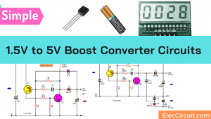
- 1.5V to 5V boost converter circuit for microcomputer
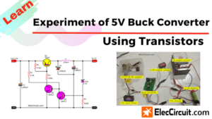
- 5V to +/- 12V boost converter circuit or higher using transistor
You should read all for more understanding.
How does the circuit works
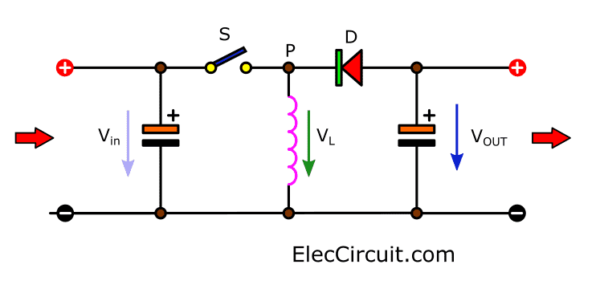
Figure 1 The basic Buck/boost converter circuit
Figure 1, when the switch (S) closed to causes a current flow through a coil (L). Then, it causes a voltage drop at L is a voltage (UL). And if SW opened, the current on L still flow continuously.
But it flows through to diode (D). It is a current collapsed rectifier as the negative voltage appears on the output. (Vout)
Both buck/boost combination is the “Buck/boost converter”, but it is not the only function to increase the voltage, we can use it for a lower voltage.
Therefore, it may be also called. Step-up/step-down converter.
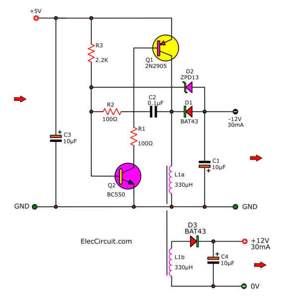
Figure 2 The circuit mixed with between the Step-up/step-down converter and the flyback converter circuit.
Keep reading: Principle of Buck DC to DC converter
Consider the circuit in Figure 2. The upper circuit or the section that has elements of the coil L1a is Buck/boost converter, that is when applying the voltage of +5 volt into this circuit causes the current flow through R3 before. The current as described above send to bias a transistor Q2 to makes Q2 conduct current.
Read also: How does a transistor circuit work
Affect the transistor Q1, causes bias because when Q2 has ready to conduct the current the resistance at collector-emitter lower. So it has a current of T1 flow to the emitter to base.
When fully integrated with Q2, Q1 gives rise to conduction. To provided current out to collector or Q1 acts as the same a switch connected the voltage source goes to drop at L1a. The voltage drop across the coil as above so equivalent power supply.
While the current gradually increased. This higher voltage through C2, R2 to a bias on the Q2 and C2 fully charged, has canceled the transfer the current to Q2. Makes Q2 lower conduct and Q1 also lower conduct too.
Keep reading: 1.5v to 5v boost converter circuit
The electric potential of L1a so changes the direction from poles above the positive, to be negative. and below that is a negative to a positive occurred rectifier or result of the current of the coil through diode D1.
To the output way one, the other one Occurred the reverse bias value with. emitter-base of Q2, makes Q2 stop and Q1 also stops or switches cut the voltage goes out from L1a.
The providing current of Buck/boost converter so compete with the basic circuit in Figure 1
Then Q2 starts conduction again and work will continue to provide current to load continuously.
We describe the operation of the transistors this much. In order to accommodate that content. The circuit as shown in Figure 1.
The principle of the Switch (S) is a continuous function.
The Circuit needs more than that. This circuit requires a regulation to control the voltage at output constant of -12 volts. So place the Zener diode D3 number ZPD13 have voltage value control 13 volts as the end of the number.
When the output voltage lower than -12 volts makes the Zener diode as above start conduct so can stop working of Q2 before timed out work, the time of conduction of Q1 and Q2 decreases. The providing voltage will lower to stage -12 volts normally.
However, there are problems of design added, is This circuit not only to the negative. But want voltage both positive and negative, Have to apply the principles of the flyback converter circuit principle is shown in Figure 3.
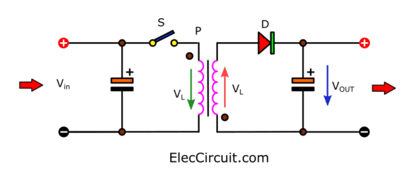
Figure 3 the basic flyback converter circuit
That’s when the switch as figure 3, will cause voltage Uin to drop at the transformer cause is voltage VL. By polarity P of the transformer has positive phase. Now the coil to the Secondary. It also can not apply voltage VL to appear to output.
Because of the Electric potential, the reverse diode is shown As black dots. electrical phase in Figure 3.
When switch S cut off, voltage polarity P backward voltage diode so apply a voltage to the output. As Vout the simple way is we will turns of coil add to L1b by Number of turns of the coil equivalent L1a.
Or is the Ratio 1: 1. The effect From switching off the circuit. that work with switch Q1 to provide the voltage to output by coil L1b.
Which acts as the secondary coil. By has diode D3 act rectifier as the output voltage of +12 volts.
May called the circuit of L1b that the Isolate converter because the voltage as above does not need to connecting common ground with the input circuit.
This circuit has 60% efficiency and should be a transformer El, the same old circuit models used there.
DC converters using small transistors
- Switch mode LED driver circuit using transistors »
- Simple 12V transistor switching power supply »
- MC34063 Switching Regulator with Buck-Boost Converter Circuits
GET UPDATE VIA EMAIL
I always try to make Electronics Learning Easy.
Related Posts

I love electronics. I have been learning about them through creating simple electronic circuits or small projects. And now I am also having my children do the same. Nevertheless, I hope you found the experiences we shared on this site useful and fulfilling.

Nice. But in market, all of these can’t be found.
Nice,But parts not easy to find in the market.
Need this type circuit as input 5v/3.6v from power bank or li-Ion battery bank and output 12v 1amp.
R1 needs to be at least 1k because max Ic(T1) = -600mA for 2N2905
a 5V zener should be used to protect T2 base because max VEB0 = 5V for BC550
Perfect for me
Hi,
You are welcome
Thank you for visiting our website.
My dad and I will keep doing this website.🌷😊