The CD4049 is another one of the most widespread CMOS inverter logic chips. This chip contains a total of six independent inverters. The CD4049 is commonly used for interfacing, simple clock generators, oscillators, or as a non-inverting buffer when connecting two of its inverters in series.

Its high-level input signal (VIH) can exceed the VCC supply voltage when used for logic-level conversions. The CD4049 is originally intended for use as a CMOS to DTL/TTL converter and is capable of directly driving two DTL/TTL loads. However, the maximum power supply must not exceed 18V.
CD4049 Features
The CD4049 is mainly used to connect CMOS to TTL, to drive current higher, to convert high-to-low or low-to-high logic levels, and for many other things.
- It can drive 2 TTL loads directly at 5.0V.
- A wide supply voltage range of 3V to 15V.
- High source and sink current.
- Input protection allows for input voltage higher than VDD.
Pinout
Buy CD4049 at Amazon.com here (affiliated link)
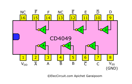
The pin assignments of DIP 16 as CD4049
Internal Schematic Diagrams
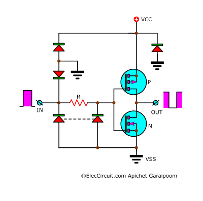
Inside each inverter gate, there are two main components: MOSFETs. They are quite efficient and faster than TTL, which uses normal transistors. However, these MOSFETs can be damaged more easily through static electricity or transient spikes; the manufacturer thus adds diodes at the input and the power supply, which increases the protection for the chip.
Both because of the protection circuit and the MOSFET itself, the CD4049 has a poor high-frequency response.
Note: Please see these circuits use CD4049 as a base::
CD4049 Circuits
Now let’s see some of the simple practical applications of the CD4049.
Simple Clock Pulse Generator
The CD4049 CMOS inverting hex buffer IC can be used to build a simple clock pulse generator circuit, as you can see below.
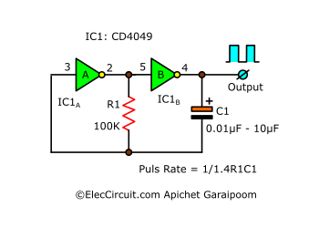
This particular circuit only requires a couple of components, a resistor and a capacitor to be exact. It can generate a pulse with a 50% duty cycle waveform. The output frequency is determined by R1 and C1 through this formula: F = 1 / (1.39 × R × C).
The power supply range for this circuit is relatively high at 3V to 12V DCV. You could also substitute the CD4049 with other CMOS ICs such as the CD4069, TC4069, and LM4069.
Here are a few related posts you might want to read:
- The simple LED Flasher using CD4011
- 60HZ CLOCK Pulse Generator using MM5369
- Simple Pulse Generator using 555 Timer
Linear 10X Amplifier
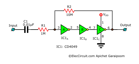
In this circuit, the inverters function as a linear amplifier, not dissimilar to an OP-AMP. From this simple formula, Gain = R2 / R1, you can choose the gain by changing the resistance of the resistors.
Phase Shift Oscillator
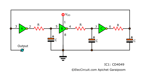
This simple phase shift oscillator generates a sine wave signal. The frequency of which is determined by the resistors and capacitors using this formula: F = 1 / (3.3 × R × C)
Square Wave Generator
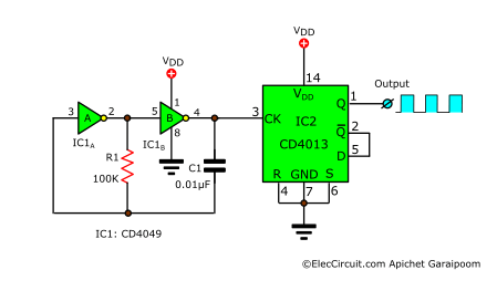
The simple clock pulse generator from above might not output the most perfect square wave. To get a better output signal, we could use a divided-by-two circuit, in this case using the D-flip-flop CD4013 chip. It will always decrease the frequency by half, hence the “divided-by-two” name.
Triangle Wave Generator
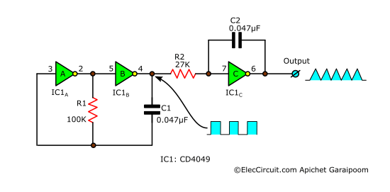
Furthermore, if you want a triangular wave generator, you could do that by adding an integrator, which consists of R2, C2, and one more inverter gate. You could also tweak R2 and C2 to achieve your exact waveform; you might be able to get a saw or sine wave from it.
Bounceless Switch Using CD4049
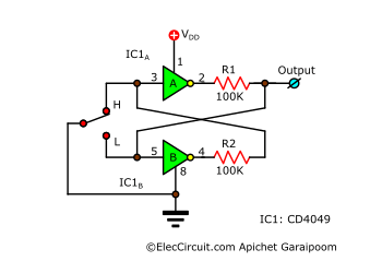
When using a normal mechanical switch with sensitive components such as a microcontroller or digital circuits in general, the switch may bounce between on and off, causing damage to the component.
This common problem is known as contact bounce, which this bounceless switch circuit can help prevent.
Conclusion
The CD4049 has many uses, and a few that we have brought up are just a small part of what it is capable of. There are still more circuits that use this chip, such as LED flasher circuits, alarm or siren circuits, and more, which we will explore at a later date. But if you want to see the CD4049 used in a specific circuit, be sure to let us know.
GET UPDATE VIA EMAIL
I always try to make Electronics Learning Easy.

I love electronics. I have been learning about them through creating simple electronic circuits or small projects. And now I am also having my children do the same. Nevertheless, I hope you found the experiences we shared on this site useful and fulfilling.


This site is facinating. Pls i will need a help in building my own inverter. I have the circuit but i need for efficient pulse generator with a variable resistor to control the trigger speed to the thyristor gate
Could you please be specific re the frequencies – I need a variable range of 1.9 MHz to 2.35 MHz. Also – an amplitude of 9 volt. What would be the average current in such a case? Thanks.
shall i use a suplly of 20v dc?? could please sugggest me to use 20v dc
i need to build a square wave generator that has 3 pots in its schematic and uses a 741 op amp IC. if i say i don’t want to use the 741 is the any IC i can use and still achieve same results?
I need to build a circuit contain a crystal oscillator square wave with 10 : 90 MHZ with 12 V input and contain all methods to controlling increase and decrease i.e up and down the output signal in MHZ to take it after that to opp orate the required Load