The MC34063 is often used as the main component in a DC-to-DC converter circuit. Even though it is not the best SMPS (Switching Mode Power Supply) IC, it’s widely used enough to be found easily on the market.
They are now very cheap and are starting to make their way into the hobby world. We often see them in many devices, such as car battery chargers, to regulate voltage from 12V to 5V converter circuits.
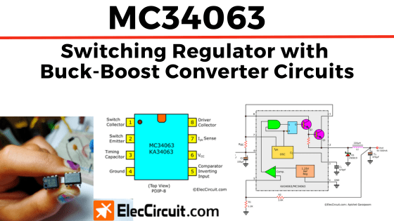
This chip can be used in buck or boost converters, inverting circuits, et cetera. It is therefore an excellent IC to use in place of LM317. Also, at a current below 1A, there is no need for external drivers, and the circuit is very simple to build.
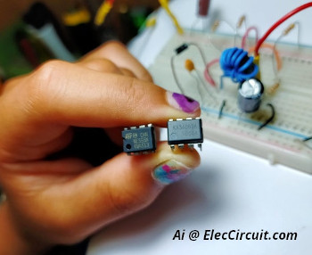
It came in the same easy-to-use PDIP-8 package as the 555 timer chip; however, it possesses features similar to a LM317. You should definitely have it stocked up; it will certainly become very handy when creating switching-mode power supplies.
What is the function of the MC34063
The MC34063 is a very useful DC-DC converter chip. We can use it as a buck converter (step-down), a boost converter (step-up), or an inverting switching regulator.
Here is the datasheet for the MC34063.
Its Feature
- Its output current capability is up to 1.5A
- Operation input voltage from 3.0V to 40V
- Current Limiting
- Adjustable Output Voltage (1.2V to 40V) with external resistors
- It can switch power at frequencies up to 100KHz.
- Efficiency about 80% to 90%
- Low Standby Current
- Precision 2% Reference
- Pb−Free Packages are Available
What is the equivalent of MC34063A?
Equivalent MC34063A DC to DC converters are MC34063A, MC33063A, SC34063A, SC33063A, KA34063,NCV33063A, CS51411, ACT4514, and TS2580.
The MC34063 Pinout
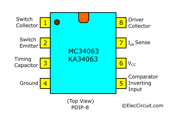
We can see the leg position of this IC below. It’s quite simple.
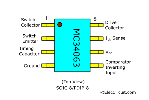
Nowadays, we prefer to use SMD devices because they are small and economical. This IC has a SOIC-8 shape, while the position of the pins remains the same as shown in the figure below.
The basic internal circuit structure
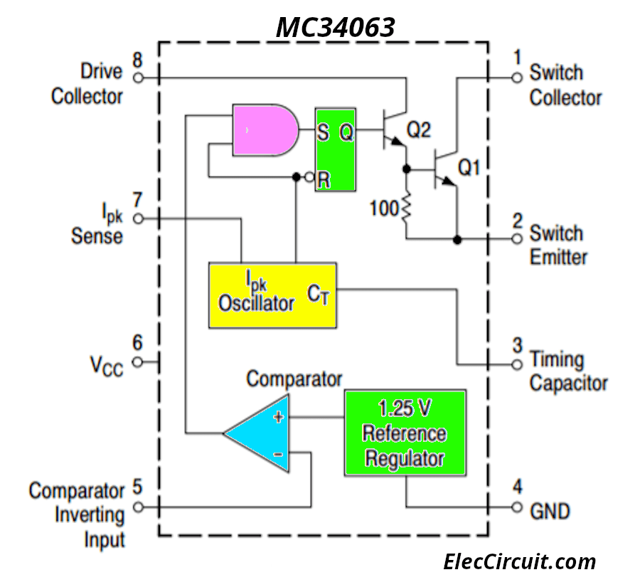
Then, see the Basic internal circuit structure below.
Cr:https://www.onsemi.com/
This chip contains multiple complex components, such as a switching system, transistor, Flip-Flop, AND gate, Oscillator, Comparator, Reference voltage, and more. It makes our work easier and more convenient.
The Q1 and Q2 are transistors run as switches at high frequencies, controlled through RS flip-flops generated by an oscillator.
In addition, the MC34063 has 8 usable pins, which are as follows:
Pins list
- Pin 6: VCC is a positive pin that must always connect the positive terminal of the source.
- Pin 4: Ground (GND) is a negative pin that must always connect the negative terminal of the source.
- Pin 1: Switch Collector connects to the power transistor (Q1).
- Pin 2: Switch Emitter drives a higher current to the ground or others.
- Pin 8: Driver Collector connects to Q2 to drive a bias current to Q1.
- Pin 3: Timing Capacitor connects to an external capacitor, the capacitance of which will determine the oscillator’s frequency up to 100kHz.
- Pin 7: Ipk Sense is for protecting against an overcurrent. When it detects voltage exceeding the Current Limit Sense Voltage (Vipk) of 340mV, it stops the oscillation.
- Pin 5: Comparator Inverting Input is to control the output voltage.
Setting the Output Voltage
Does the 1.25V reference regulator block seem familiar to you? Because yes, the LM317 also has one. We can use it together with the comparator and two external resistors to monitor the voltage and maintain stability.
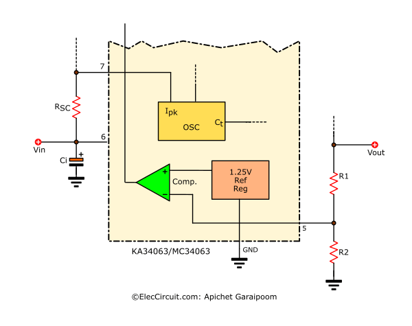
We will use R1 and R2 to set the MC34063’s output voltage and calculate the resistance of both resistors using the following formula:
Vout = 1.25 V x {1 + R2/R1}
The formula is the same as the one used for the LM317, and the internal structure of both of them also contains the 1.25V reference voltage and the comparator. In the block diagram, the comparators’ output is connected to the AND gates’ input.
Or you may pick the resistance of R1 and R2 for your desired output voltage from the list below.
1.43V : R1 = 470Ω, R2 = 68Ω
1.47V : R1 = 470Ω, R2 = 82Ω
1.47V : R1 = 390Ω, R2 = 68Ω
1.51V : R1 = 330Ω, R2 = 68Ω
1.51V : R1 = 390Ω, R2 = 82Ω
1.52V : R1 = 470Ω, R2 = 100Ω
1.53V : R1 = 390Ω, R2 = 82Ω
1.56V : R1 = 330Ω, R2 = 82Ω
1.57V : R1 = 270Ω, R2 = 68Ω
1.57V : R1 = 470Ω, R2 = 120Ω
1.57V : R1 = 390Ω, R2 = 100Ω
1.59V : R1 = 390Ω, R2 = 100Ω
1.60V : R1 = 240Ω, R2 = 68Ω
1.63V : R1 = 330Ω, R2 = 100Ω
1.63V : R1 = 270Ω, R2 = 82Ω
1.64V : R1 = 390Ω, R2 = 120Ω
1.64V : R1 = 220Ω, R2 = 68Ω
1.65V : R1 = 470Ω, R2 = 150Ω
1.66V : R1 = 390Ω, R2 = 120Ω
1.68V : R1 = 240Ω, R2 = 82Ω
1.71V : R1 = 330Ω, R2 = 120Ω
1.71V : R1 = 270Ω, R2 = 100Ω
1.72V : R1 = 220Ω, R2 = 82Ω
1.72V : R1 = 180Ω, R2 = 68Ω
1.73V : R1 = 470Ω, R2 = 180Ω
1.73V : R1 = 390Ω, R2 = 150Ω
1.76V : R1 = 390Ω, R2 = 150Ω
1.77V : R1 = 240Ω, R2 = 100Ω
1.81V : R1 = 270Ω, R2 = 120Ω
1.82V : R1 = 150Ω, R2 = 68Ω
1.82V : R1 = 330Ω, R2 = 150Ω
1.82V : R1 = 180Ω, R2 = 82Ω
1.83V : R1 = 390Ω, R2 = 180Ω
1.84V : R1 = 470Ω, R2 = 220Ω
1.86V : R1 = 390Ω, R2 = 180Ω
1.88V : R1 = 240Ω, R2 = 120Ω
1.89V : R1 = 470Ω, R2 = 240Ω
1.93V : R1 = 330Ω, R2 = 180Ω
1.93V : R1 = 150Ω, R2 = 82Ω
1.94V : R1 = 270Ω, R2 = 150Ω
1.96V : R1 = 390Ω, R2 = 220Ω
1.97V : R1 = 470Ω, R2 = 270Ω
1.99V : R1 = 390Ω, R2 = 220Ω
2.02V : R1 = 390Ω, R2 = 240Ω
2.03V : R1 = 240Ω, R2 = 150Ω
2.06V : R1 = 390Ω, R2 = 240Ω
2.08V : R1 = 330Ω, R2 = 220Ω
2.10V : R1 = 220Ω, R2 = 150Ω
2.12V : R1 = 390Ω, R2 = 270Ω
2.13V : R1 = 470Ω, R2 = 330Ω
2.16V : R1 = 330Ω, R2 = 240Ω
2.16V : R1 = 390Ω, R2 = 270Ω
2.19V : R1 = 240Ω, R2 = 180Ω
2.23V : R1 = 470Ω, R2 = 390Ω
2.25V : R1 = 150Ω, R2 = 120Ω
2.27V : R1 = 270Ω, R2 = 220Ω
2.27V : R1 = 330Ω, R2 = 270Ω
2.29V : R1 = 470Ω, R2 = 390Ω
2.29V : R1 = 180Ω, R2 = 150Ω
2.31V : R1 = 390Ω, R2 = 330Ω
2.36V : R1 = 270Ω, R2 = 240Ω
2.37V : R1 = 390Ω, R2 = 330Ω
2.40V : R1 = 240Ω, R2 = 220Ω
2.44V : R1 = 390Ω, R2 = 390Ω
2.50V : R1 = 470Ω, R2 = 470Ω
2.57V : R1 = 390Ω, R2 = 390Ω
2.61V : R1 = 220Ω, R2 = 240Ω
2.65V : R1 = 330Ω, R2 = 390Ω
2.66V : R1 = 240Ω, R2 = 270Ω
2.73V : R1 = 330Ω, R2 = 390Ω
2.74V : R1 = 470Ω, R2 = 560Ω
2.75V : R1 = 150Ω, R2 = 180Ω
2.76V : R1 = 390Ω, R2 = 470Ω
2.78V : R1 = 270Ω, R2 = 330Ω
2.78V : R1 = 220Ω, R2 = 270Ω
2.84V : R1 = 390Ω, R2 = 470Ω
2.92V : R1 = 180Ω, R2 = 240Ω
2.96V : R1 = 270Ω, R2 = 390Ω
2.97V : R1 = 240Ω, R2 = 330Ω
3.03V : R1 = 330Ω, R2 = 470Ω
3.05V : R1 = 390Ω, R2 = 560Ω
3.06V : R1 = 270Ω, R2 = 390Ω
3.06V : R1 = 470Ω, R2 = 680Ω
3.08V : R1 = 150Ω, R2 = 220Ω
3.13V : R1 = 220Ω, R2 = 330Ω
3.14V : R1 = 390Ω, R2 = 560Ω
3.18V : R1 = 240Ω, R2 = 390Ω
3.25V : R1 = 150Ω, R2 = 240Ω
3.28V : R1 = 240Ω, R2 = 390Ω
3.37V : R1 = 330Ω, R2 = 560Ω
3.43V : R1 = 270Ω, R2 = 470Ω
3.43V : R1 = 390Ω, R2 = 680Ω
3.43V : R1 = 470Ω, R2 = 820Ω
3.47V : R1 = 220Ω, R2 = 390Ω
3.50V : R1 = 150Ω, R2 = 270Ω
3.54V : R1 = 180Ω, R2 = 330Ω
3.55V : R1 = 390Ω, R2 = 680Ω
3.70V : R1 = 240Ω, R2 = 470Ω
3.82V : R1 = 180Ω, R2 = 390Ω
3.83V : R1 = 330Ω, R2 = 680Ω
3.84V : R1 = 270Ω, R2 = 560Ω
3.88V : R1 = 390Ω, R2 = 820Ω
3.91V : R1 = 470Ω, R2 = 1K
3.92V : R1 = 220Ω, R2 = 470Ω
3.96V : R1 = 180Ω, R2 = 390Ω
4.00V : R1 = 150Ω, R2 = 330Ω
4.02V : R1 = 390Ω, R2 = 820Ω
4.17V : R1 = 240Ω, R2 = 560Ω
4.33V : R1 = 150Ω, R2 = 390Ω
4.36V : R1 = 330Ω, R2 = 820Ω
4.40V : R1 = 270Ω, R2 = 680Ω
4.43V : R1 = 220Ω, R2 = 560Ω
4.44V : R1 = 470Ω, R2 = 1.2K
4.46V : R1 = 390Ω, R2 = 1K
4.50V : R1 = 150Ω, R2 = 390Ω
4.51V : R1 = 180Ω, R2 = 470Ω
4.63V : R1 = 390Ω, R2 = 1K
4.79V : R1 = 240Ω, R2 = 680Ω
5.04V : R1 = 330Ω, R2 = 1K
5.05V : R1 = 270Ω, R2 = 820Ω
5.10V : R1 = 390Ω, R2 = 1.2K
5.11V : R1 = 220Ω, R2 = 680Ω
5.14V : R1 = 180Ω, R2 = 560Ω
5.17V : R1 = 150Ω, R2 = 470Ω
5.24V : R1 = 470Ω, R2 = 1.5K
5.30V : R1 = 390Ω, R2 = 1.2K
5.52V : R1 = 240Ω, R2 = 820Ω
5.80V : R1 = 330Ω, R2 = 1.2K
5.88V : R1 = 270Ω, R2 = 1K
5.91V : R1 = 220Ω, R2 = 820Ω
5.92V : R1 = 150Ω, R2 = 560Ω
5.97V : R1 = 180Ω, R2 = 680Ω
6.04V : R1 = 470Ω, R2 = 1.8K
6.06V : R1 = 390Ω, R2 = 1.5K
6.32V : R1 = 390Ω, R2 = 1.5K
6.46V : R1 = 240Ω, R2 = 1K
6.81V : R1 = 270Ω, R2 = 1.2K
6.92V : R1 = 150Ω, R2 = 680Ω
6.93V : R1 = 330Ω, R2 = 1.5K
6.94V : R1 = 180Ω, R2 = 820Ω
7.02V : R1 = 390Ω, R2 = 1.8K
7.10V : R1 = 470Ω, R2 = 2.2K
7.33V : R1 = 390Ω, R2 = 1.8K
7.50V : R1 = 240Ω, R2 = 1.2K
8.07V : R1 = 330Ω, R2 = 1.8K
8.08V : R1 = 150Ω, R2 = 820Ω
8.19V : R1 = 270Ω, R2 = 1.5K
8.30V : R1 = 390Ω, R2 = 2.2K
8.43V : R1 = 470Ω, R2 = 2.7K
8.68V : R1 = 390Ω, R2 = 2.2K
9.06V : R1 = 240Ω, R2 = 1.5K
9.58V : R1 = 330Ω, R2 = 2.2K
9.77V : R1 = 220Ω, R2 = 1.5K
9.90V : R1 = 390Ω, R2 = 2.7K
10.03V : R1 = 470Ω, R2 = 3.3K
10.37V : R1 = 390Ω, R2 = 2.7K
10.63V : R1 = 240Ω, R2 = 1.8K
11.25V : R1 = 150 Ω, R2 = 1.2K
11.44V : R1 = 270Ω, R2 = 2.2K
11.48V : R1 = 330Ω, R2 = 2.7K
11.67V : R1 = 180Ω, R2 = 1.5K
11.83V : R1 = 390Ω, R2 = 3.3K
12.40V : R1 = 390Ω, R2 = 3.3K
12.71V : R1 = 240Ω, R2 = 2.2K
13.75V : R1 = 330Ω, R2 = 3.3K
15.31V : R1 = 240Ω, R2 = 2.7K
16.25V : R1 = 150Ω, R2 = 1.8K
16.53V : R1 = 270Ω, R2 = 3.3K
16.59V : R1 = 220Ω, R2 = 2.7K
18.44V : R1 = 240Ω, R2 = 3.3K
19.58V : R1 = 150Ω, R2 = 2.2K
20.00V : R1 = 220Ω, R2 = 3.3K
23.75V : R1 = 150Ω, R2 = 2.7K
24.17V : R1 = 180Ω, R2 = 3.3K
28.75V : R1 = 150Ω, R2 = 3.3K
The RSC
It is a max-current limit resistor; it can ensure the safety of the circuit and increase the efficiency of oscillation.
The RSC is placed between pin 6 (Vin) and pin 7 to limit the inductors’ maximum current.
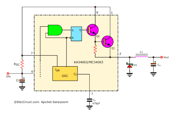
If the RSC has a resistance of 0.33 ohms and the current flowing through it exceeds 1A, it will cause the voltage drop across RSC (pin 7) to be around 330mV, thus stopping the oscillator.
Connecting Internal Driver and Power Transistors
Next, let’s see the external component configuration needed for both the buck converter and boost converter setup. We will connect these components to the driver transistor (Q2) and power transistor (Q1) inside the chip.
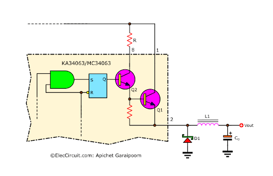
The buck converter setup for this chip will be able to supply a high amount of current, which is similar to a common collector transistor configuration. The setup is quite simple; firstly, connect pin 2 or E of Q1 to the ground. Next, connect pin 8 to V+ via the resistor; this will allow the driver current in to the Q2. And lastly, connect D1 and L1 to pin 1.
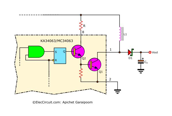
On the other hand, in the boost converter setup, the Q1 will be in a common emitter configuration. Also, it will be able to withstand a higher voltage but supply less current. The pin 2 is connected to the ground, and pin 1 is connected to D1 and L1, which is the opposite of the boost converter setup.
Increasing The Current
Normally, this chip is capable of supplying a current of up to 1A. However, if we need more current, such as 2A, 3A, or higher, we will need to add in a power transistor.
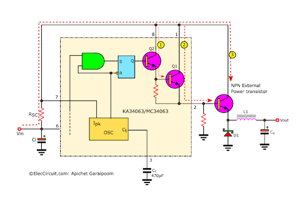
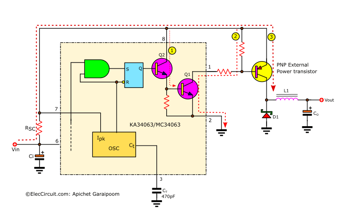
According to my experience, the PNP transistor configuration has a higher efficiency than the NPN’s. And because the PNP uses a common emitter configuration, it can also supply a higher amount of current.
Example MC34063 Circuits
Let’s take a look at some of the example circuits that use the MC34063. As previously mentioned, the MC34063 circuits can be divided into the following three main categories.
- Buck Converter
- Boost Converter
- Invertering Switching Regulator
Buck Converter
Simple Buck Converter Circuit
We will start with the Simple 5V Buck Converter Circuit or the 5V 500mA Switching Regulator Circuit. It can be placed in the buck converter category, hence the name. This circuit has a higher efficiency than a linear regulator.
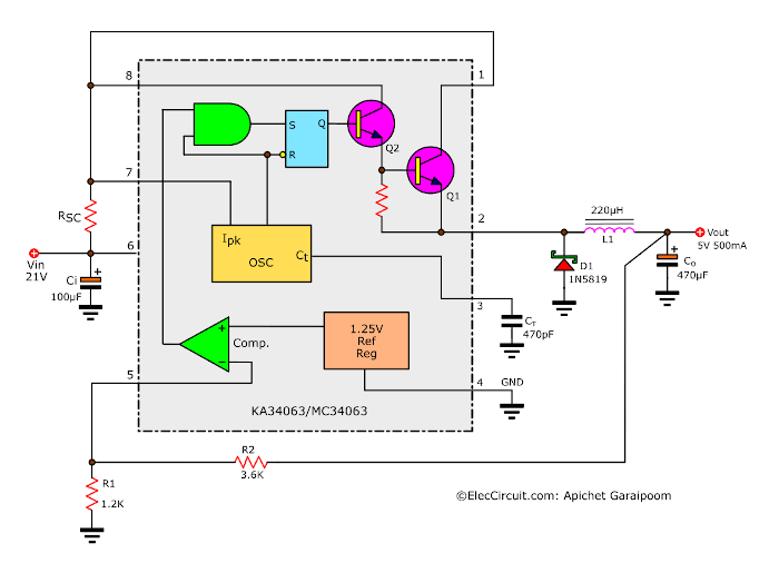
For instance, if supplied with a Vin of 21V 100mA, it will have enough capacity to drive a 500mA load.
2A Buck Converter Using PNP Transistor
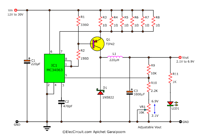
2.1V to 6.9V 2A switching power supply circuit using MC34063 and TIP42 PNP transistor.
Boost converter
3.7V to 5V Boost/Step-up DC Converter Circuit
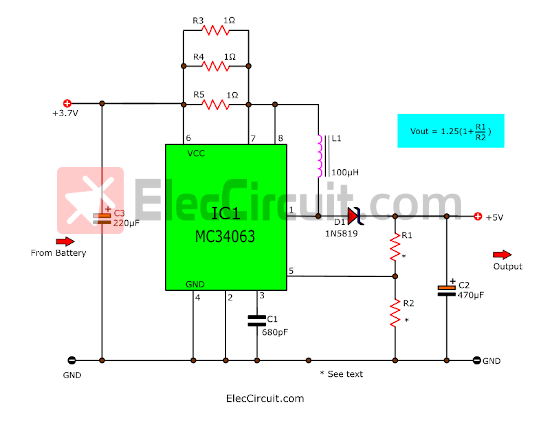
Here is a 3.7V to 5V boost converter or step-up switching circuit using MC34063 and a few parts,1N5819,100uH. For 200mA-300mA of load current.
4V to 12V DC Boost Converter
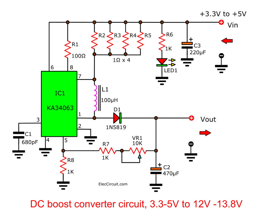
This 4V to 12V DC Boost Converter Circuit can convert an input voltage (3.3V-5V) to higher output voltage(12V-13.8V) at 500mA of current.
12V to 28V Boost DC Converter Circuit
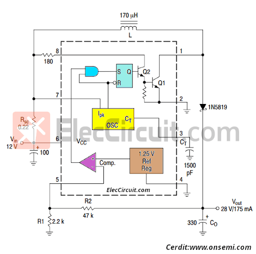
This boost switching regulator circuit can boost a 12V battery to 28V output at 170mA current.
12V Battery Voltage Regulator Circuit
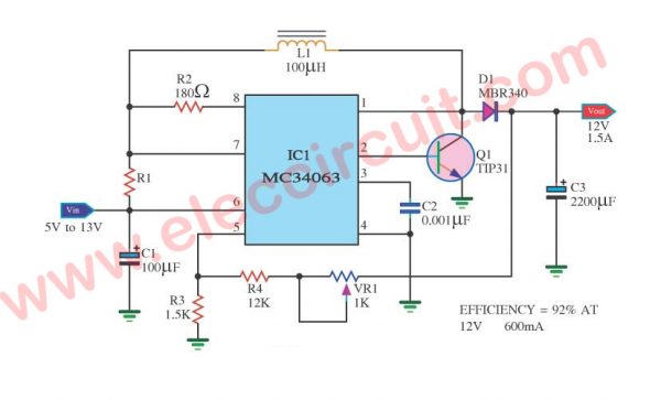
This circuit will maintain the output at 12V 600mA even when the input varies between 5V and 13V. It is a switching mode regulator circuit that consists of only a few components.
The MC34063 chip is connected to the VCC by its pin 6 and connected to the GND by its pin 4. Also, a 100uF capacitor filters unwanted noise from the power supply. Pin 2 is connected to the base of external boost current transistors (Q1) to the ground.
The C2 is connected to Pin 3 as the timing capacitor to set the switching speed (oscillator) of the circuit.
Pin 5 is an inverting input of the comparator inside the chip, while the non-inverting input connects to the 1.25V reference voltage regulator inside the chip.
There are two resistors connecting to the inverting pin (pin 5); these decide the gain of the OP-AMP comparator through the formula: VOUT=1.25V (1 + R4/R3).
Since we want the output to be 12V, the R3 needs to be 1.5K and the R4’s 12K. Nevertheless, there is still the VR1 to fine-tune the output voltage.
Invertering Switching Regulator
The ideal of these regulators is very simple: it inverts the input voltage from positive to negative, and vice versa.
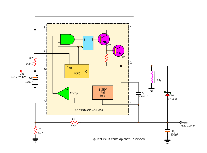
In this example circuit, it will convert from a 5V positive input to a -12V negative output. It is just a type of buck converter, but with the polarity of D1 and Co inverted.
Conclusion
As you can see, the MC34063 is one simple and versatile SMPS (Switching Mode Power Supply) chip. Also, if we very much want to increase the maximum current, we can replace the power transistor with the MOSFET instead, since it has a higher efficiency. I will discuss those circuits next time; please stay tuned.
GET UPDATE VIA EMAIL
I always try to make Electronics Learning Easy.
Related Posts

I love electronics. I have been learning about them through creating simple electronic circuits or small projects. And now I am also having my children do the same. Nevertheless, I hope you found the experiences we shared on this site useful and fulfilling.


Very good…
Thanks for your feedback.
How to increase current up to 3A output?
Next time, I will introduce a circuit that can supply a higher current with MOSFET.